which is an argument that "fpga_pio" is badly implemented or that PIO is unsuitable for FPGA impls. Real silicon does not need to use a shitton of LUT4s to implement this logic and it can be done much more efficiently and closes timing at higher clocks (as we know since PIO will run near a GHz)
> If you’re thinking about using it in an FPGA, you’d be better off skipping the PIO and just implementing whatever peripherals you want directly using RTL.
Because it does what it does so well, I use the PIO as the design study comparison point. This requires taking a critical view of its architecture. Such a review doesn't mean its design is bad - but we try to take it apart and see what we can learn from it. In the end, there are many things the PIO can do that the BIO can't do, and vice-versa. For example, the BIO can't do the PIO's trick of bit-banging DVI video signals; but, the PIO isn't going to be able to protocol processing either.
In terms of area, the larger area numbers hold for both an ASIC flow as well as the FPGA flow. I ran the design through both sets of tools with the same settings, and the results are comparable. However, it's easier to share the FPGA results because the FPGA tools are NDA-free and everyone can replicate it.
That being said, I also acknowledge in the article that it's likely there are clever optimizations in the design of the actual PIO that I did not implement. Still, barrel shifters are a fairly expensive piece of hardware whether in FPGA or in ASIC, and the PIO requires several of them, whereas the BIO only has one. The upshot is that the PIO can do multiple bit-shifts in a single clock cycle, whereas the BIO requires several cycles to do the same amount of bit-shifting. Again, neither good or bad - just different trade-offs.
I've done some fun stuff in PIO, in particular the NRZI bit stuffing for USB (12Mbps max). That's stretching it to its limit. Clearly there will be things for which BIO is much better.
I suspect that a variant of BIO could probably do DVI by optimizing for that specific use case (in particular, configuring shifters on the output FIFO), but I'm not sure it's worth the lift.
When considering the space of possibilities, I focused on applications that I could see there being actual product sold that rely upon the feature. The problem with DVI is that while it's a super-clever demo, I don't see volume products going to market relying upon that feature. The moment you connect to an external monitor, you're going to want an external DRAM chip to run the sorts of applications that effectively utilize all those pixels. I could be wrong and mis-judged the utility of the demo but if you do the analysis on the bandwidth and RAM available in the Baochip, I feel that you could do a retro-gaming emulator with the chip, but you wouldn't, for example, be replacing a video kiosk with the chip. Running DOOM on a TV would be cool, but also, you're not going to sell a video game kit that just runs DOOM and nothing else.
The good news is there's plenty of room to improve the performance of the BIO. If adoption is robust for the core, I can make the argument to the company that's paying for the tape-outs to give me actual back-end resources and I can upgrade the cores to something more capable, while improving the DMA bandwidth, allowing us to chase higher system frequencies. But realistically, I don't see us ever reaching a point where, for example, we're bit-banging USB high speed at 480Mbps - if not simply because the I/Os aren't full-swing 3.3V at that point in time.
You may be right about not much scope for DVI in volume products. I should be clear I'm just playing with RP2350 because it's fun. But the limitation you describe really has more to do with the architectural decision to use a framebuffer. I'm interested in how much rendering you can get done racing the beam, and have come to the conclusion it's quite a lot. It certainly includes proportional fonts, tiles'n'sprites, and 4bpp image decompression (I've got a blog post in the queue). Retro emulators are a sweet spot for sure (mostly because their VRAM fits neatly in on-chip SRAM), but I can imagine doing a kiosk.
Definitely agree that bit-banging USB at 480Mbps makes no sense, a purpose-built PHY is the way to go.
The BIO should also be able to overclock. It won't overclock as well as the PIO, for sure - the PIO stores its code in flip-flops, which performance scales very well with elevated voltages. The BIO uses a RAM macro, which is essentially an analog part at its heart, and responds differently to higher voltages.
That being said, I'm pretty confident that the BIO can run at 800MHz for most cases. However, as the manufacturer I have to be careful about frequency claims. Users can claim a warranty return on a BIO that fails to run at 700MHz, but you can't do the same for one that fails to run at 800MHz - thus whenever I cite the performance of the BIO, I always stick it at the number that's explicitly tested and guaranteed by the manufacturing process, that is, 700MHz.
Third-party overclockers can do whatever they want to the chip - of course, at that point, the warranty is voided!
The 25MHz number I cite as the performance expectation is "relaxed": I don't want to set unrealistic expectations on the core's performance, because I want everyone to have fun and be happy coding for it - even relatively new programmers.
However, with a combination of overclocking and optimization, higher speeds are definitely on the horizon. Someone on the Baochip Discord thought up a clever trick I hadn't considered that could potentially get toggle rates into the hundreds of MHz's. So, there's likely a lot to be discovered about the core that I don't even know about, once it gets into the hands of more people.
On rp2350 it is pio (wait for clock) -> pio (read address bus) -> dma (addr into lower bits of dma source for next channel) -> dma (Data from SRAM to PIO) -> pio (write data to data bus) chain and it barely keeps up.
The PRUs really get a bunch right. Very specifically, the ability to broadside dump the ENTIRE register file in a single cycle from one PRU to the other is gigantic. It's the single thing that allows you to transition the data from a hard real-time domain to a soft real-time domain and enables things like the industrial Ethernet protocols or the BeagleLogic, for example.
One thing jumped out here - I assumed CISC inside PIO had a mental model of "one instruction by cycle" and thus it was pretty easy to reason about the underlying machine (including any delay slots etc...).
For this RISC model using C, we are now reasoning about compiled code which has a somewhat variable instruction timing (1-3 cycles) and that introduces an uncertainty - the compiler and understanding its implementation.
I think this means that the PIO is timing-first, as timing == waveform where BIO is clarity-first with C as the expression and then explicit hardware synchronization.
I like both models! I am wondering about the quantum delays however that are being used to set the deadlines - here, human derived wait delays are utilized knowledge of the compiled instructions to set the timing.
Might there not be a model of 'preparing the next hardware transaction' and then 'waiting for an external synchronization' such as an external signal or internal clock, so we don't need to count the instruction cycles so precisely. On the external signal side, I guess the instruction is 'wait for GPIO change' or something, so the value is immediately ready (int i = GPIO_read_wait_high(23) or something) and the external one is doing the same, but synchronizing (GPIO_write_wait_clock( 24, CLOCK_DEF)) as an alternative to the explicit quantum delays.
This might be a shadow register / latch model in more generic terms - prep the work in shadow, latch/commit on trigger.
Anyway, great work Bunnie!
That being said - one nice thing about the BIO being open source is you can run the verilog design in Verilator. The simulation shows exactly how many cycles are being used, and for what. So for very tight situations, the open source RTL nature of the design opens up a new set of tools that were previously unavailable to coders. You can see an example of what it looks like here: https://baochip.github.io/baochip-1x/ch00-00-rtl-overview.ht...
Of course, there's a learning curve to all new tools, and Verilator has a pretty steep curve in particular. But, I hope people give the Verilator simulations a try. It's kind of neat just to be able to poke around inside a CPU and see what it's thinking!
The C compiler support is a relatively recent addition, mostly to showcase the possibilities of doing high-level protocol offloading into the BIO, and the tooling benefits of sticking with a "standard" instruction set.
Btw I am curious what about edge cases. Maybe I have missed that from the article but what is the size of the FIFO?
Or the more dangerous part that is you have complex to determine timing now for complex cases like each reqd from FIFO is and ISR and you have until the next read from the FIFO amount of instructions otherwise you would stall the system and that looks to me too hard to debug.
The deadlock possibilities with the FIFO are real. It is possible to check the "fullness" of a FIFO using the built-in event subsystem, which allows some amount of non-blocking backpressure to be had, but it does incur more instruction overhead.
Have some on the way! Can't wait!
Ah yes, the good ol “we solved the C problem by turning it into four other problems” pipeline
My point is, maybe this is one of those designs that blow up in FPGA. Or maybe the open source version of the PIO is simply not as area efficient as the rpi version?
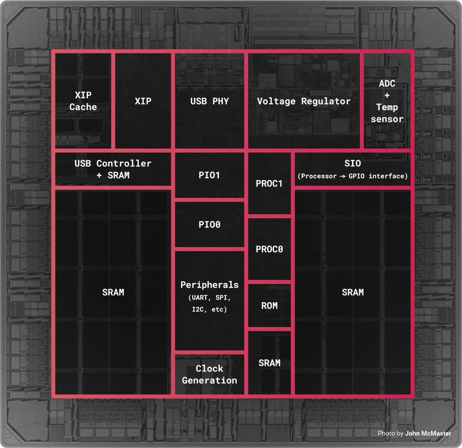
But even on the real RP2040, PIO is not small.
Take a look at the annotated die shot [0]. The PIO blocks are notably bigger than the PROC blocks.
[0] https://assets.raspberrypi.com/static/floorplan@2x-a25341f50...